(I have corrected this post as to give the wrong impression)
Having done further programming with the Buffalo DAC, I realized that the register address values I used for the OPUS code are pehaps wrongly coded in 8-bit format where the I2C protocol of the Arduino Wire library is based on 7-bit register addresses.
The code as it is works with volume, oversampling filter selection and even filter choice, even though I can't tell the filters apart (but a high frequency test tone with young people proved that they can tell filters apart)
This means that the OPUS DAC code for the WM8741, should be reviewed for the address value.
Monday, October 15, 2012
Wednesday, March 31, 2010

Monday, March 22, 2010
Another Musiland 01 Mini mod
 I removed the capacitors I installed in the backside of the board (see here). Instead I removed the capacitor from the switching supplies -power traces cut- (220 uf) and replaced the capacitors of the linear regulators (10 uf). Another advantage of getting the mini...
Saturday, March 20, 2010


Monday, March 15, 2010
Comparing Noise Figures in Linear Regulators
Just like phase noise in clocks, it is difficult to compare noise values among linear regulators because there is no common ground in specifying noise figures. Some companies report noise density, others RMS V noise, and yet others % of Vout. The frequency range for the reported noise figures also varies from company to company.
The LT1763 familiy is a favorite for audio projects because it has low noise figures. Among linear regulators it is probably universally preferred by audio diy aficionados.
In order to compare other regulators to this benchmark device, I decided to calculate the Vrms noise in each of the fequency ranges provided by the chart. The Vrms noise is basically the product of the noise density times the frequency delta.
The results is shown in the graph below. Total Vrms = 23.2 uVrms for the frequency range 10Hz to 100KHz. This approximation is very close to the specified value of 20 uVrms.
I then looked as the specified noise of several common regulators and matched the values to the corresponding value of the LT1763 device.
A couple of observations: The LM340 is actually very good, in fact better than the beloved LM317 according to spec. The LM723 seems of lower noise than the LT1763, at least in the reported frequency range.


Here is a very good paper from TI explaining noise in linear regulators: [link]
According to the paper,
The LT1763 familiy is a favorite for audio projects because it has low noise figures. Among linear regulators it is probably universally preferred by audio diy aficionados.
In order to compare other regulators to this benchmark device, I decided to calculate the Vrms noise in each of the fequency ranges provided by the chart. The Vrms noise is basically the product of the noise density times the frequency delta.
The results is shown in the graph below. Total Vrms = 23.2 uVrms for the frequency range 10Hz to 100KHz. This approximation is very close to the specified value of 20 uVrms.
I then looked as the specified noise of several common regulators and matched the values to the corresponding value of the LT1763 device.
A couple of observations: The LM340 is actually very good, in fact better than the beloved LM317 according to spec. The LM723 seems of lower noise than the LT1763, at least in the reported frequency range.


We can approximate the total noise Vrms for the 10Hz-100KHz interval by noticing that each frequency range contributes a percentage of the total noise. In the case of the LT1763, we notice that the 10Hz-10KHz range contributes about half of the total 10Hz-100KHz noise. The table below compares all the regulators in the 10Hz-100KHz range.

Here is a very good paper from TI explaining noise in linear regulators: [link]
According to the paper,
"The dominant source of noise in an LDO is usually theUnfortunately, it is not easy to access the bandgap output line in most integrated regulators...
bandgap. In most cases this is solved by adding a large
low-pass filter (LPF) to the bandgap output so that none
of the noise makes it into the gain stage."
Thursday, March 11, 2010
TPA's AC1 FAQ
Not an Arduino, but based on a cousin of the ATMega168 with built-in USB. Of course totally incompatible with the Arduino development tools. But if you are familiar with Arduino, you'd easily navigate this device.
More pictures over at TPA's website


Instructions for loading (burning) firmware into FEMTO:
2- Copy libusb0.dll from usb directory to bin directory: copy the file C:\Program Files\Atmel\Flip 3.4.1\usb\libusb0.dll to C:\Program Files\Atmel\Flip 3.4.1\bin. Make sure you copy the file because it is needed on both directories
3- Insert FEMTO and do the following sequence:
a- Push HWD button
b- Push RST button
c- Release RST button
d- Release HWD button
4- At this point Windows will recognize the device ( FEMTO) and will guide you though the driver installation. 5- Select manual installation and you point the path to: C:\Program Files\Atmel\Flip 3.4.1\usb
6- Start FLIP
7- Start USB communication: Settings->Communication->USB
8- Select device: Device-Select->AT90USB162
9- Select hex file: File->Load Hex File->filename.hex
10- Click Run
Saturday, February 27, 2010
Programming Buffalo DAC: Review of Arduino I2C
Is is fairly simple to use Arduino to program a DAC such as the ESS Sabre32. After you connect the appropriate signals (wires) from Arduino to the Buffalo board, you follow the tutorial sketches (in Arduino the programs are called sketches) to set up the main code and use the Arduino I2C functions to write values into the registers of the DAC.
In Arduino, the I2C protocol is supported by the "Wire library" and the functions are the following:
- begin() - Join the I2C bus as a masterdevice
- begin(address) - Join the I2C bus as a slave device
- requestFrom(address, count) - Tell device that a request will follow
- beginTransmission(address) - Tell device as address that data transmission will start
- endTransmission()- Tell device that transmission is ended
- send() - Send data (one byte at a time)
- byte available() - Queries number of bytes available for retrieval
- byte receive() - Retrieve (read) bytes from device
- onReceive(handler) - The function to perform when slave receive a transmission
- onRequest(handler) - The function to perform when slave receives a request
Before you do anything, Arduino joins the I2C bus as a master device with
begin()
The following code will write one value into one register:
beginTransmission(0x80); // Address of DAC is hex 80
send(0x01); // Address of register is hex 1
send(0x00); // Value into register is hex 0
endTransmission;
Hex is hexadecimal notation. It is more convenient to write in hex notation rather than binary notation. Most data sheets give you register address value in hex and register value in binary. You can use any notation in your code but you have to indicate which notation.
You can convert binary to hex with one of many online tools such as this.
The following code sends one value to 4 registers. This example is typical for setting volume. The same value is assigned to all the internal DACs. Say for example the volume control of the DAC is 1/4 db and you want to set a -10 db volume. The value to use is -40 (you don't have to specify which notation because the default is decimal notation), and assume the registers to control the volume are registers 1 through 4
beginTransmission(0x80); // Address of DAC is hex 80
send(0x01); // Address of register 1 is hex 1
send(40); // Value into register 40
send(0x02); // Address of register 2 is hex 2
send(0x02); // Address of register 2 is hex 2
send(40); // Value into register 40
send(0x03); // Address of register 3 is hex 3
send(0x03); // Address of register 3 is hex 3
send(40); // Value into register 40
send(0x04); // Address of register 4 is hex4 send(40); // Value into register 40
endTransmission;
That's it.
Update (October, 12, 2010): I just implemented and tested the basic code to control the Buffalo II DAC's volume. However, I couldn't program multiple registers within a single beginTransmission and endTransmission pair as shown above. I had to program each register with beginTransmission...endTransmission separately. You can see the code here.
Monday, February 22, 2010
Audiophile HQCD
Finally got my copy of Bondy Chiu's audiophile recording from Hong Kong. It was sold out over Christmas...
HQCD is a higher quality pressing by using lens quality plastic and silver allow first developed for the now dead HD-DVD.
Bondy Chiu (you can hear her music here) is a Hong Kong-based artist that with Ken Poon (his blog is Design with Sound), a recording engineer and audiophile has created perhaps the first mass-market Audiophile CD.

The CD sounds very good, and if you got friends in Hong Kong, can be purchased for around HK$ 160.

Wednesday, February 17, 2010
Programming Buffalo II DAC: I2C Isolation
As extreme care has been afforded to reduce noise on Buffalo II, perhaps it would be also prudent to implement the I2C isolation solution to prevent any noise sneaking through an external microprocessor such as Arduino on the I2C lines.
Note: a reader alerted me that the on-board microprocessor goes to sleep after setting up the registers of the DAC. In such case, there should be no additional noise from the on-board microprocessor. However, when the microprocessor is sleeping, only an interrupt can wake it up. If one uses the Arduino as the external microprocessor, some of the code may not be interrupt based, for example polling IR remote signals. So, if the microprocessor is doing more than just setting up the registers at power-on, in general it is not a good idea to put the microprocessor to sleep. Therefore some isolation in the i2c lines would be a welcomed noise avoidance implementation.
Analog Devices magnetic coupling devices has a solution for this task: The ADum1250. Previous observations here indicate that this is the best solution.

The pull up resistors on side 2 (right side) in the diagram are already implemented in Arduino (inside the uP and enabled in software).

The pull-up resistors on side 1 (left side) I believe are already implemented in Buffalo II as R14 and R15? -Need to confirm with the designers.

Note: a reader alerted me that the on-board microprocessor goes to sleep after setting up the registers of the DAC. In such case, there should be no additional noise from the on-board microprocessor. However, when the microprocessor is sleeping, only an interrupt can wake it up. If one uses the Arduino as the external microprocessor, some of the code may not be interrupt based, for example polling IR remote signals. So, if the microprocessor is doing more than just setting up the registers at power-on, in general it is not a good idea to put the microprocessor to sleep. Therefore some isolation in the i2c lines would be a welcomed noise avoidance implementation.
Analog Devices magnetic coupling devices has a solution for this task: The ADum1250. Previous observations here indicate that this is the best solution.
The ADuM1250/ADuM12511 are hot swappable digital isolators with nonlatching, bidirectional communication channels compatible with I2C® interfaces. This eliminates the need for splitting I2C signals into separate transmit and receive signals for use with standalone optocouplers.The application note indicates that side 1 (left) should be used for the device (the DAC) and side 2 for the I2C bus (Arduino)
The ADuM1250 provides two bidirectional channels, supporting a complete isolated I2C interface. The ADuM1251 provides one bidirectional channel and one unidirectional channel for those applications where a bidirectional clock is not required.
Both the ADuM1250 and ADuM1251 contain hot swap circuitry to prevent glitching data when an unpowered card is inserted onto an active bus.

The pull up resistors on side 2 (right side) in the diagram are already implemented in Arduino (inside the uP and enabled in software).

The pull-up resistors on side 1 (left side) I believe are already implemented in Buffalo II as R14 and R15? -Need to confirm with the designers.

Thursday, February 11, 2010
Buffalo II DAC Clock Jitter at 0.1 psec RMS?
In the previous post we found that the Crystek oscillator used in the Buffalo II DAC is very good, better than the typical oscillator found in many hi end audio equipment, but obviously not as good as the best money can buy. The phase noise graphs look sort close to each other, but how much different are they?
Audiophiles are accustomed to hear jitter values in terms of pico-seconds (psec) RMS, and many oscillators are spec'ed at 1 psec jitter. We know that phase noise is another way to measure jitter, and that jitter RMS values represent the area under the curve. One must realize that the graph is in logarithm scale resulting in large differences even though the curves are sort of close to each other.
Analog Devices has an excellent tutorial on understanding jitter values

You can use the formulas to calculate jitter RMS from phase noise data, but there are easy to use on-line tools that calculate jitter RMS from data you find in datasheets. One such tool is the Phase Noise Calculator from www.jittertime.com (a consultancy on the topic of jitter)
So lets calculate the jitter RMS value for each of the oscillators we compared in the previous post.
We find the data points in the graph and enter them in the tool as shown:
 The result is 0.446 psec. (if you are wondering why the result is less than the sum of the jitter in each segment, is because they add as Root Sum-of-Squares)
This value agrees with the value is the specification ( typically 0.5 psec). We do the same for the other curves and we find the following:
Those are BIG differences when we convert to jitter RMS values. the Wenzel measures 75 femto seconds!. The Crystek 950 measures the expected half a psec; but the typical oscillator measure 30 psec?. But wait a minute, aren't those oscillators spec'ed at 1 psec?.
Lets looks at the specification of the oscillator found in Buffalo I: Crystek c33xx. The spec says: Jitter RMS: 12KHz-80MHz: 0.5 psec. Notice that the jitter is measured after 12 KHz whereas the phase noise plots we see for the better parts starts at 10 Hz. If we instead measure the Jitter RMS for the Crystek 950 shown in the graph with the same scale, of 12 KHz to 80 MHz, we get the value of 0.13 psec.
I used the numbers found in the spec for an 80MHz oscillator and got 0.115 psec for 12KHz to 80MHz. The best spec in the datasheet is for the 100MHz clock with a jitter value of 0.094 psec RMS (12KHz-80MHz). Maybe the custom clock Crystek is making for TPA has better phase noise values than what is stated in the specifications. (Update: according to Brian of TPA, the phase noise specification for their parts is the same as the standard parts)
Thus:
What offset frequency interval is used for audio to calculate jitter? I don't think there are standards in audio, but for other applications there are standards. This article cites two standards:
If we take a previous datasheet of the Crystek 950 clock and compare it with the current datasheet, we see that the "close-in" phase noise (closer to the crystal frequency) has increased and that "broad band" phase noise (away from the crystal frequency).
It seems that the engineers at Crystek focused on improving the broadband phase noise values and were willing to tradeoff the close-in phase noise. This implies that broadband phase numbers (or the "noise floor" of the oscillator) is a more important value than close-in noise (at least for the market that this crystal is intended to be used, -which I am sure it is NOT DIY DAC boards :-))

Perhaps it depends on the application
According to tutorial from Analog Devices,
YET another data point for frequency interval
A reader alerted me to an excellent AES paper on jitter for audio components, available for free from Wolfson Micro. There, the authors propose a "baseband" value of 100Hz to 40K Hz
If we use these frequency values we obtain (via the handy online jitter calculation tool) the following jitter values:
Unfortunately most of the research on the effect of phase noise revolve around digital telecommunication, where the frequency is in the 100s of MHz. There clock jitter determines the SNR and effectively the bandwidth of the devices, and the phase noise value that is important is the broadband phase noise.
So what is the effect of phase noise in audio?
According to this AES paper by Bruno Putzeys (Hypex, Grimm Audio) it is just noise.
I also took a look at other implementations of the ESS DAC and what kind of clock they use. It seems that only DIY versions can "afford" the high-end clock... Also note that the ESS evaluation board uses a "standard" crystal, rather than a clock (or so it looks like)

Eastern Electric DAC

Audiophiles are accustomed to hear jitter values in terms of pico-seconds (psec) RMS, and many oscillators are spec'ed at 1 psec jitter. We know that phase noise is another way to measure jitter, and that jitter RMS values represent the area under the curve. One must realize that the graph is in logarithm scale resulting in large differences even though the curves are sort of close to each other.
Analog Devices has an excellent tutorial on understanding jitter values

You can use the formulas to calculate jitter RMS from phase noise data, but there are easy to use on-line tools that calculate jitter RMS from data you find in datasheets. One such tool is the Phase Noise Calculator from www.jittertime.com (a consultancy on the topic of jitter)
So lets calculate the jitter RMS value for each of the oscillators we compared in the previous post.
Buffalo II oscillator
We find the data points in the graph and enter them in the tool as shown:
 The result is 0.446 psec. (if you are wondering why the result is less than the sum of the jitter in each segment, is because they add as Root Sum-of-Squares)
This value agrees with the value is the specification ( typically 0.5 psec). We do the same for the other curves and we find the following:
- Crystek 950 (Buffalo II): 0.446 psec
- Wenzel oscillator: 0.075 psec
- Typical Oscillator (Buffalo I): 29.9 psec
Those are BIG differences when we convert to jitter RMS values. the Wenzel measures 75 femto seconds!. The Crystek 950 measures the expected half a psec; but the typical oscillator measure 30 psec?. But wait a minute, aren't those oscillators spec'ed at 1 psec?.
Lets looks at the specification of the oscillator found in Buffalo I: Crystek c33xx. The spec says: Jitter RMS: 12KHz-80MHz: 0.5 psec. Notice that the jitter is measured after 12 KHz whereas the phase noise plots we see for the better parts starts at 10 Hz. If we instead measure the Jitter RMS for the Crystek 950 shown in the graph with the same scale, of 12 KHz to 80 MHz, we get the value of 0.13 psec.
I used the numbers found in the spec for an 80MHz oscillator and got 0.115 psec for 12KHz to 80MHz. The best spec in the datasheet is for the 100MHz clock with a jitter value of 0.094 psec RMS (12KHz-80MHz). Maybe the custom clock Crystek is making for TPA has better phase noise values than what is stated in the specifications. (Update: according to Brian of TPA, the phase noise specification for their parts is the same as the standard parts)
Thus:
- Clock for Buffalo I: 0.5 psec RMS (12KHz-80MHz)
- Clock for Buffalo II: 0.115 psec RMS (12KHz-80MHz)
What offset frequency interval is used for audio to calculate jitter? I don't think there are standards in audio, but for other applications there are standards. This article cites two standards:
As an example, SONET uses a frequency offset of 12kHz to 20MHz from the carrier signal to integrate the area under the phase noise plot to measure phase jitter. Fiber Channel uses a frequency offset of 637kHz to 10MHz from the carrier signal to integrate the area under the phase noise plot to measure phase jitter.According to Analog Devices,
It is a little tricky to specify the bandwidth over which phase noise should be integrated in order to calculate the jitter which will actually be observed when that clock signal is used to clock a converter. There are many variables which are seldom known with accuracy – such as the inherent bandwidth of the sample clock circuit on the converter. Also, it is very difficult to actually measure the broadband phase noise of a clock signal beyond an offset of a few MHz. ... For a true "broadband" jitter calculation some assumptions and simplifications must be made. One assumption made by ADIsimCLK, for example, is that the upper offset integration limit is one-half the clock frequency. The lower offset integration limit is assumed to be between 100 Hz and 1 kHz.What frequency interval matters then?
If we take a previous datasheet of the Crystek 950 clock and compare it with the current datasheet, we see that the "close-in" phase noise (closer to the crystal frequency) has increased and that "broad band" phase noise (away from the crystal frequency).
It seems that the engineers at Crystek focused on improving the broadband phase noise values and were willing to tradeoff the close-in phase noise. This implies that broadband phase numbers (or the "noise floor" of the oscillator) is a more important value than close-in noise (at least for the market that this crystal is intended to be used, -which I am sure it is NOT DIY DAC boards :-))

Perhaps it depends on the application
According to tutorial from Analog Devices,
- Close-in phase noise limits the frequency resolution
- Broadband phase noise reduces SNR
YET another data point for frequency interval
A reader alerted me to an excellent AES paper on jitter for audio components, available for free from Wolfson Micro. There, the authors propose a "baseband" value of 100Hz to 40K Hz
If we use these frequency values we obtain (via the handy online jitter calculation tool) the following jitter values:
- 1.6 psec or 1600 fsec for a c33xx class clock (100Hz-40KHz)
- 0.046 psec or 46 fsec for a 950 class clock (100Hz-40KHz)
Unfortunately most of the research on the effect of phase noise revolve around digital telecommunication, where the frequency is in the 100s of MHz. There clock jitter determines the SNR and effectively the bandwidth of the devices, and the phase noise value that is important is the broadband phase noise.
So what is the effect of phase noise in audio?
According to this AES paper by Bruno Putzeys (Hypex, Grimm Audio) it is just noise.
I also took a look at other implementations of the ESS DAC and what kind of clock they use. It seems that only DIY versions can "afford" the high-end clock... Also note that the ESS evaluation board uses a "standard" crystal, rather than a clock (or so it looks like)

Eastern Electric DAC

Clock in Buffalo II DAC

According the Brian in this post, the clock in Buffalo II is not only the top-of-the line product from Crystek, but a custom made model with even better specifications.
For those with sharp eyes, the photo of the Buffalo II prototype has a 50 ppm (temperature stability) clock, but the production models will have a 20 ppm part.Temperature stability is related to the quality of the quartz crystal used in the clock. It is therefore safe to assume that this will also improve the jitter figures.
But how good is Crystek's best oscillator?
There is a white paper by Crystek showing "phase noise" curves for the 950 oscillator and compared to a typical oscillator. I copied the charts and overlaid them together. In addition I took a look at the specifications of a ultra low phase noise Wenzel oscillator and a Rubidium oscillator and plotted the data on the same chart. The Rubidium is a "$900 low cost" version. Perhaps they are best at frequency stability over a long period of time and therefor they cost so much. The Wenzel oscillators are the lowest phase noise you can find and are used in High Energy Physics and Radio Astronomy applications. If you work for NASA or CERN, maybe you can borrow one of these clocks and hook it up to your DAC :-).
Update: NEL AE-X3A3 oscillators have better specifications than Crystek 950. The NEL Oven controlled oscillator is even lower noise (not sure how much they cost)
(Clik for larger image)

How is Ultralow Phase Noise Achieved?
According to the author in the Crystek white paper,
"A commodity oscillator is nothing more than an ASIC and a quartz crystal blank. In most cases, it does not even have an internal bypass capacitor. The crystal blank is an AT-cut strip with Q of about 25 K to 45 K. This low Q limits the close-in phase noise. The ASIC with all its transistors limits the floor noise to about -150 dBc/Hz. On the other hand, the true ultralow phase noise oscillator uses a discrete high-performance oscillator topology with a packaged crystal with a Q greater than 70 K for excellent close-in phase noise. The discrete oscillator topology establishes the SNR, and hence the floor is lower than -160 dBc/Hz. Therefore, superior performance is obtained with very high Q crystals and a good discrete topology."How is the Phase-Noise graph obtained? The chart is one half of the power-frequency distribution of the variation from ideal. Instruments are available to generate such charts.

Quarts oscillators is an "old" technology. "Fundamentals of Quartz Oscillators", an application note from HP from the late '70s is a good read.

The Buffalo II DAC: Best Bang-for-Buck
(Update, Nov. 2010: I've developed Arduino code to control the Buffalo DAC. Check my other blog: www.hifiduino.wordpress.com)
TwistedPearAudio Released the Buffalo II DAC
TwistedPearAudio Released the Buffalo II DAC
This is the 3rd TPA iteration for the top of the line ESS DAC. The first iteration was for the ESS 9008 (24bit) DAC and the second and third are for the ESS 9018 (32bit).
Although it is priced at $249, the ESS DAC includes a spdif receiver, a high speed ASRC and a 32-bit DAC. In Addition, the Buffalo II includes a top-of-the line, ultra low jitter clock from Crystek and a ultra-low noise shunt regulator for the analog section of the DAC.
I think Buffalo II is the new bang-for-buck leader. If we compare a comparable OPUS DAC offering we have the following:
- Opus DAC (WM8741): $75
- Opus Spdif Receiver (WM8804): $75
- Metronome (ASRC): $75
- Upgrade Clock (you must mod yourself): $30
- Upgrade analog regulation (e.g. Placid, and mod yourself): $40
Total: $295
To be fair, the OPUS does not require an output stage and associated power supply, and the Buffalo II requires an output stage.
In-depth comparison between Buffalo I DAC (ESS 9008) and Buffalo II DAC (ESS 9018) also shows that the new DAC is a better deal than the old DAC (Buffalo I photo scraped from "buyer of board #93 without permission)
BUFFALO I DIGITAL TO ANALOG CONVERTER

BUFFALO II DIGITAL TO ANALOG CONVERTER

Buffalo I ---------------Buffalo II
Total: 53.75 ---------------------------Total: 115.11
Difference: $61.36I believe the Buffalo I sold for $169. If we add the price differential for the 4-layer board, and the time spent designing and prototyping and testing the new board, we can easily reach the $80 price difference between the old Buffalo and Buffalo II.
Ah! I forgot the ultra-low noise dual analog regulator, you get that for FREE! (Expect to pay $60 to $120 for two shunt low noise regulators from 3rd parties)
Update:
- There are a couple of dozen additional components in the back side of the PCB
- The clock is a custom made 20 ppm (standard is 25-50 ppm) model for TPA
COMPARISON WITH BUFFALO 32S
I believe the main difference between Buffalo II and Buffalo 32s (aside from having the I/V stage in a separate board) is the analog supply. It appears (from pictures, I don't have the boards and there are no schematics for Buffalo 32s) the analog supply of Buffalo 32s is similar to the one found in Buffalo I.
Buffalo 32s analog supply: based on two LM4971 single opamps


Wednesday, February 10, 2010
Buffalo II Specification and FAQ
This post is to summarize information I find elsewhere
EXTERNAL POWER SUPPLY REQUIREMENTS
POWER SUPPLY CURRENT [link]

POWER SUPPLY VOLTAGE [link]
The Buff II board has a single PS connection. Because it feeds both the on board LT1763 regulators and the AVCC dual shunt regulator, it must comply to the design of the AVCC dual shunt:
According the the ESS Sabre DAC white paper, AVCC is specified as follows:

"Also of note, although the AVCC header has four pins, only three are used by our AVCC module.
The AVCC module does not use the DVCC pin. It is there as a convenience to any who might want to use an ESS demo board style AVCC supply (where DVCC is a VREF). Our AVCC module uses its own low noise VREF, not DVCC."
Note: Buffalo I also derived the AVCC from the DVCC. In the case you wish to replicate such AVCC implementation, you can tap into DVCC as reference and VD will be powering the buffer opamp:

Normal Operating Conditions [link]
(This is one board, there is slight variations between boards)
VD=5V. Notice that one LED is brighter than the other. According to TPA this is perfectly normal.
AVCC1=3.523V, VCC2=3.5626V

VD=5.5V. Notice that the LEDs' brightness is more uniform.
AVCC1=3.556V, AVCC2=3.554V

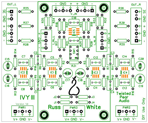
The shut regulator board can also be installed on the back side of the Buffalo II board (It will get on the way if you are stacking above IVY III)

ON BOARD LINEAR REGULATORS

DUAL MONO INSTALLATION
Latest diagram posted at diyaudio
DIMENSIONS


EXTERNAL POWER SUPPLY REQUIREMENTS
POWER SUPPLY CURRENT [link]

POWER SUPPLY VOLTAGE [link]
The Buff II board has a single PS connection. Because it feeds both the on board LT1763 regulators and the AVCC dual shunt regulator, it must comply to the design of the AVCC dual shunt:
- Vmin=5V
- Vmax=5.5V (The AVCC shunt regulator is optimized to this voltage)
According the the ESS Sabre DAC white paper, AVCC is specified as follows:
- Minimum: 1.8V
- Nominal: 3.3V (DNR= -132db)
- Maximum: 4.0V (DNR> -133db) - see footnote 17 of paper

"Also of note, although the AVCC header has four pins, only three are used by our AVCC module.
The AVCC module does not use the DVCC pin. It is there as a convenience to any who might want to use an ESS demo board style AVCC supply (where DVCC is a VREF). Our AVCC module uses its own low noise VREF, not DVCC."
Note: Buffalo I also derived the AVCC from the DVCC. In the case you wish to replicate such AVCC implementation, you can tap into DVCC as reference and VD will be powering the buffer opamp:

Normal Operating Conditions [link]
(This is one board, there is slight variations between boards)
VD=5V. Notice that one LED is brighter than the other. According to TPA this is perfectly normal.
AVCC1=3.523V, VCC2=3.5626V

VD=5.5V. Notice that the LEDs' brightness is more uniform.
AVCC1=3.556V, AVCC2=3.554V

The shut regulator board can also be installed on the back side of the Buffalo II board (It will get on the way if you are stacking above IVY III)

ON BOARD LINEAR REGULATORS

- There are 3 linear regulators LT 1763. Two are 3.3 V and one is variable set to 1.2V
- Noise level: 20uVrms 10Hz to 100KHz (meaning you can't do better than this even if you feed it a cleaner supply). For more information on regulator noise see this post.
- Regulator Vin max=20V (5.5V max is specified because the same input traces feed the the shunt AVCC regulator which is designed for 5.5V max)
- Comments by Russ on the use of LT1763 as regulator for the Crystek clock: "The reason the LT1763 is a good fit for the clock we use is because that clock in essence has a form of local regulation and decoupling internally."
- 195 ohm each output
DUAL MONO INSTALLATION
Latest diagram posted at diyaudio
DIMENSIONS
- Buffalo II board: 2" x 3.3". This is the same size as the other modules such as OPUS, COD, Buffalo I, etc.
- IVY III: From the layout it appears it is a double size board: 4" x 3.3"
- Supplied Standoffs: .5" base standoffs. Inter-board standoffs (not included with the Buffalo II board are .625")


Monday, February 8, 2010
Musiland Driver 1.082: Fast vs Precision
A reader sent me some measurements on the I2S lines with the latest driver. The first picture is with Fast Mode and the second picture is with Precision Mode. I think the error of 4 Hz is probably due to probe or calibration as the theoretical deviation in fast mode is 17 Hz (The measurement shows 21 Hz deviation)


In addition, he measured the LRCK signal in an oscilloscope. The waveform looks very clean. Note: device is powered with an external low noise regulator (not USB power)

44.1K Waveform

Saturday, February 6, 2010
Programming the WM8804

I'm going to attempt to use the WM8804 SPDIF receiver in software mode. A quick look at the datasheet shows that there are 30 registers to program!. I've done an extensive search in the internet and there are no projects involving using this part in software mode. In fact, it seems it is not very easy to program.
But first lets explore this device in a bit more detail.
According to the manufacturer, the WM8804 has the lowest intrinsic jitter of any commercial spdif receiver. In addition, it provides large immunity against incoming jitter.
Lets explore why the WM8804 is immune to incoming jitter.
Conventional spdif receivers utilize a PLL to lock into the signal. Devices such as the very popular CS8412/14/16 operate this way. A PLL generates an initial clock with a VCO (voltage controlled oscillator) and compares the phase of that clock with an incoming clock. The error in phase results in a voltage that is feed back to the VCO until the output clock "locks" unto the input clock. According to an AES paper:
Popular S/PDIF receiver chips like the Yamaha YM3623B and Crystal CS8412 are NOT crystal controlled but rather recover the necessary clock from internal Phase Locked Loops (PLL) locked onto the incoming data stream. The simple two pin can crystals often seen directly attached to '3623's and '8412's are optional. The 3623 uses the crystal clock to quickly lock onto the S/PDIF signal. The 8412 uses the crystal clock to determine and display the sample rate and jitter level of the S/PDIF signal. Both parts ignore the local crystal clock once locked onto the S/PDIF signal.
Higher end parts will use a sample rate converter to further clean the jitter. Both TI and Cirrus have spdif receivers with built in ASRCs It is noted that the use of ASRC is controversial in high end audio (there are camps on both sides)
According to Wolfson in their white paper:
The goal here is to synchronize a clock generated from a PLL and high quality oscillator to incoming S/PDIF data stream. This is different to usual approach of using a PLL to recover a clock from the S/PDIF data stream, which inherently has to track the jitter to maintain lock.The white paper gives the technical details, but suffice to say that it is essentially a PLL followed by a re-clocker (not a sample rate converter) with a time based derived from the crystal. I have a post comparing the difference between re-clocking and sample rate conversion here.
Measurements by Wolfson shows the WM8804 compared with another commercial part
The following picture shows the jitter performance of the WM8804 with incoming signal having 5UI of jitter injected in the input sdif signal (5UI is 5x163nsec for 48K sample frequency). Result: 51.7 psec (period jitter RMS) which is the same as the spec'ed intrinsic jitter of the device (50 psec)

The following picture shows the jitter performance of a competitive device spec'ed with 150 psec of intrinsic jitter. The result is 334psec (period jitter RMS)

To be fair, 5UI of jitter which translates into 800 nsec which is a HUGE amount of jitter. The lowly Apple Airport Express was measured by Stereophile to have a "respectably low 258ps of jitter" in the spdif output. Thus in real life, I think the relevant measure is intrinsic jitter in which the Wolfson part excels at 50 psec
Here is the WM8804 Implementation by TwistedPearAudio:

Subscribe to:
Posts (Atom)